Busque con el número de pieza junto con el fabricante o la descripción
AOB11N60 |


| Part Number | AOB11N60 |
| Manufacturer | INCHANGE |
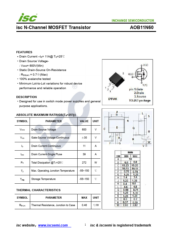
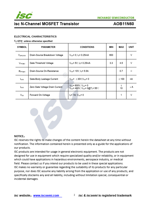
| Description | ·Designed for use in switch mode power supplies and general purpose applications. ABSOLUTE MAXIMUM RATINGS(Ta=25℃) SYMBOL PARAMETER VALUE UNIT VDSS Drain-Source Voltage 600 V VGS Gate-Source Voltage-Continuous ±30 V ID Drain Current-Continuous 11 A IDM Drain Current-Single Pluse 39 A PD Total Dissipation @TC=25℃ 272 W TJ Max. Operat. |
| Features |
·Drain Current –ID= 11A@ TC=25℃ ·Drain Source Voltage- : VDSS= 600V(Min) ·Static Drain-Source On-Resistance : RDS(on) = 0.7Ω(Max) ·100% avalanche tested ·Minimum Lot-to-Lot variations for robust device performance and reliable operation DESCRIPTION ·Designed for use in switch mode power supplies and general purpose applications. ABSOLUTE MAXIMUM RATINGS(Ta=25℃) SYMBOL PARAMETER VALUE UNIT VDSS Drain-Source Voltage 600 V VGS Gate-Source Voltage-Continuous ±30 V ID Drain Current-Continuous 11 A IDM Drain Current-Single Pluse 39 A PD Total Dissipation @TC=25℃ 272 W TJ M. |
| Datasheet |
PDF 249.12KB |
| Distributor | Stock | Price | Buy |
|---|
AOB11N60 |
| Part Number | AOB11N60 |
| Manufacturer | Alpha & Omega Semiconductors |
| Title | 11A N-Channel MOSFET |
| Description | The AOB11N60 has been fabricated using an advanced high voltage MOSFET process that is designed to deliver high levels of performance and robustness in popular ACDC applications.By providing low RDS(on), Ciss and Crss along with guaranteed avalanche capability this device can be adopted quickly into. |
| Features | C ID IDM IAR EAR EAS dv/dt PD TJ, TSTG TL Symbol RθJA RθCS RθJC Single plused avalanche energy G Peak diode recovery dv/dt TC=25° C Power Dissipation B Derate above 25oC Junction and Storage Temperature Range Maximum lead temperature for soldering purpose, 1/8" from case for 5 seconds Thermal Characteristics Parameter Maximum Junction-to-Ambient A,D Maximum Case-to-sink Maximum Junction-to-Case A. |
| No. | Parte # | Fabricante | Descripción | Hoja de Datos |
|---|---|---|---|---|
| 1 | AOB1100L |

INCHANGE |
N-Channel MOSFET |

|
| 2 | AOB1100L |

Freescale |
100V N-Channel Rugged Planar MOSFET |

|
| 3 | AOB1100L |
Alpha & Omega Semiconductors |
100V N-Channel Rugged Planar MOSFET |

|
| 4 | AOB11C60 |
Alpha & Omega Semiconductors |
11A N-Channel MOSFET |

|
| 5 | AOB11S60 |
Alpha & Omega Semiconductors |
Power Transistor |

|
| 6 | AOB11S60 |

INCHANGE |
N-Channel MOSFET |

|
| 7 | AOB11S60L |
Alpha & Omega Semiconductors |
Power Transistor |

|
| 8 | AOB11S65 |

Freescale |
Power Transistor |

|
| 9 | AOB11S65 |
Alpha & Omega Semiconductors |
Power Transistor |

|
| 10 | AOB11S65 |

INCHANGE |
N-Channel MOSFET |

|