Busque con el número de pieza junto con el fabricante o la descripción
74ALVCH16841 |


| Part Number | 74ALVCH16841 |
| Manufacturer | nexperia (https://www.nexperia.com/) |
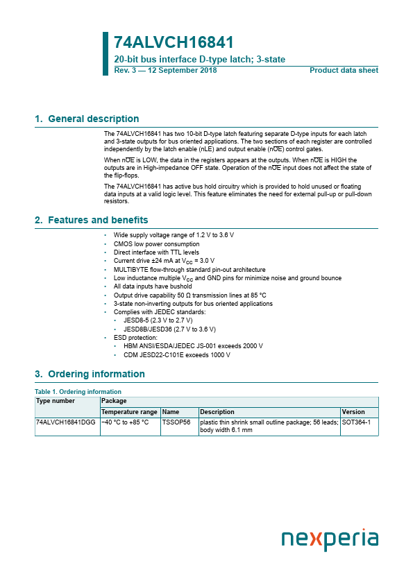
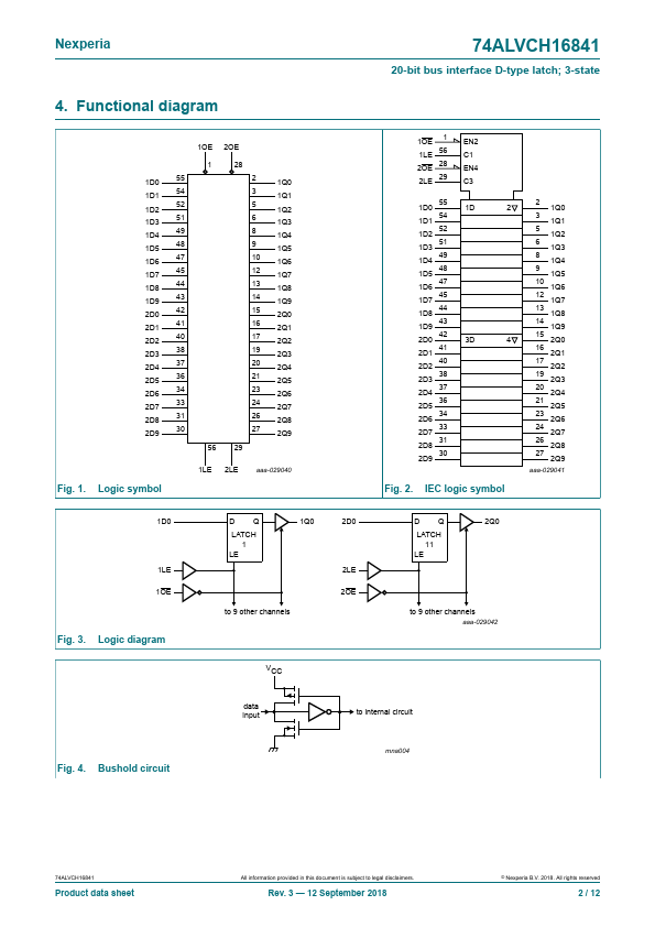
| Description | The 74ALVCH16841 has two 10-bit D-type latch featuring separate D-type inputs for each latch and 3-state outputs for bus oriented applications. The two sections of each register are controlled independently by the latch enable (nLE) and output enable (nOE) control gates. When nOE is LOW, the data in the registers appears at the outputs. When nOE is HIGH the . |
| Features |
• Wide supply voltage range of 1.2 V to 3.6 V • CMOS low power consumption • Direct interface with TTL levels • Current drive ±24 mA at VCC = 3.0 V • MULTIBYTE flow-through standard pin-out architecture • Low inductance multiple VCC and GND pins for minimize noise and ground bounce • All data inputs have bushold • Output drive capability 50 Ω transmission lines at 85 °C • 3-state non-inverting outputs for bus oriented applications • Complies with JEDEC standards: • JESD8-5 (2.3 V to 2.7 V) • JESD8B/JESD36 (2.7 V to 3.6 V) • ESD protection: • HBM ANSI/ESDA/JEDEC JS-001 exceeds 2000 V • CDM JESD. |
| Datasheet |
PDF 204.86KB |
| Distributor | Stock | Price | Buy |
|---|
74ALVCH16841 |
| Part Number | 74ALVCH16841 |
| Manufacturer | NXP |
| Title | 20-bit bus interface D-type latch |
| Description | The 74ALVCH16841 has two 10-bit D-type latch featuring separate D-type inputs for each latch and 3-State outputs for bus oriented applications. The two sections of each register are controlled independently by the latch enable (nLE) and output enable (nOE) control gates. When nOE is LOW, the data in. |
| Features |
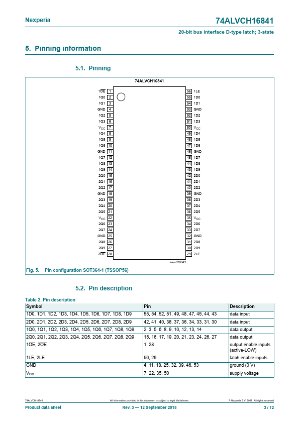
• Wide supply voltage range of 1.2V to 3.6V • Complies with JEDEC standard no. 8-1A • Wide supply voltage range of 1.2V to 3.6V • CMOS low power consumption • Direct interface with TTL levels • MULTIBYTETM flow-through standard pin-out architecture • Low inductance multiple VCC and GND pins for minimum noise and ground bounce PIN CONFIGURATION 1OE 1Q0 1Q1 GND 1Q2 1Q3 VCC 1Q4 1Q5 1Q6 GND 1Q7 1Q8 . |
| No. | Parte # | Fabricante | Descripción | Hoja de Datos |
|---|---|---|---|---|
| 1 | 74ALVCH16841DGG |

nexperia |
20-bit bus interface D-type latch |

|
| 2 | 74ALVCH16843 |

NXP |
18-bit bus-interface D-type latch |

|
| 3 | 74ALVCH16843 |

nexperia |
18-bit bus-interface D-type latch |

|
| 4 | 74ALVCH16843DGG |

nexperia |
18-bit bus-interface D-type latch |

|
| 5 | 74ALVCH16821 |

NXP |
20-bit bus-interface D-type flip-flop |

|
| 6 | 74ALVCH16821 |

nexperia |
20-bit bus-interface D-type flip-flop |

|
| 7 | 74ALVCH16821DGG |

nexperia |
20-bit bus-interface D-type flip-flop |

|
| 8 | 74ALVCH16823 |

NXP |
18-bit bus-interface D-type flip-flop |

|
| 9 | 74ALVCH16823 |

nexperia |
18-bit bus-interface D-type flip-flop |

|
| 10 | 74ALVCH16823DGG |

nexperia |
18-bit bus-interface D-type flip-flop |

|