Busque con el número de pieza junto con el fabricante o la descripción
74ALVCH16821 |


| Part Number | 74ALVCH16821 |
| Manufacturer | nexperia (https://www.nexperia.com/) |
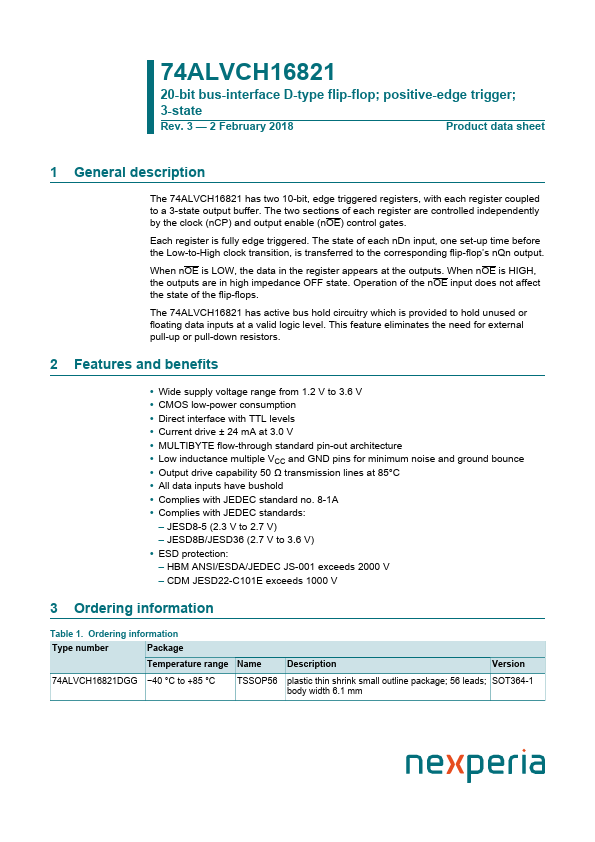
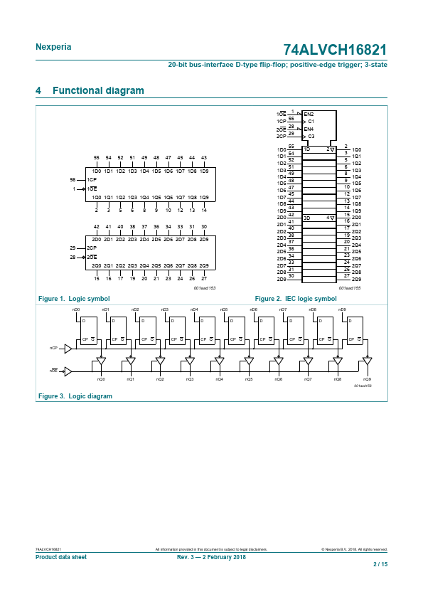
| Description | The 74ALVCH16821 has two 10-bit, edge triggered registers, with each register coupled to a 3-state output buffer. The two sections of each register are controlled independently by the clock (nCP) and output enable (nOE) control gates. Each register is fully edge triggered. The state of each nDn input, one set-up time before the Low-to-High clock transition,. |
| Features |
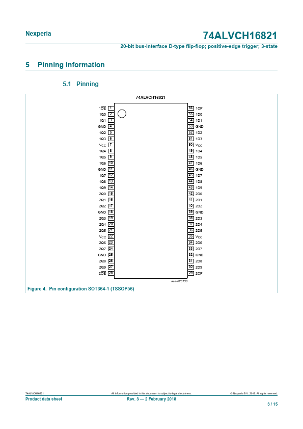
• Wide supply voltage range from 1.2 V to 3.6 V • CMOS low-power consumption • Direct interface with TTL levels • Current drive ± 24 mA at 3.0 V • MULTIBYTE flow-through standard pin-out architecture • Low inductance multiple VCC and GND pins for minimum noise and ground bounce • Output drive capability 50 Ω transmission lines at 85°C • All data inputs have bushold • Complies with JEDEC standard no. 8-1A • Complies with JEDEC standards: – JESD8-5 (2.3 V to 2.7 V) – JESD8B/JESD36 (2.7 V to 3.6 V) • ESD protection: – HBM ANSI/ESDA/JEDEC JS-001 exceeds 2000 V – CDM JESD22-C101E exceeds 1000 V 3. |
| Datasheet |
PDF 188.24KB |
| Distributor | Stock | Price | Buy |
|---|
74ALVCH16821 |
| Part Number | 74ALVCH16821 |
| Manufacturer | NXP |
| Title | 20-bit bus-interface D-type flip-flop |
| Description | The 74ALVCH16821 has two 10-bit, edge triggered registers, with each register coupled to a 3-State output buffer. The two sections of each register are controlled independently by the clock (nCP) and Output Enable (nOE) control gates. Each register is fully edge triggered. The state of each D input,. |
| Features |
• Wide supply voltage range of 1.2V to 3.6V • Complies with JEDEC standard no. 8-1A • Current drive ± 24 mA at 3.0 V • CMOS low power consumption • Direct interface with TTL levels • MULTIBYTETM flow-through standard pin-out architecture • Low inductance multiple VCC and ground pins for minimum noise and ground bounce DESCRIPTION The 74ALVCH16821 has two 10-bit, edge triggered registers, with ea. |
| No. | Parte # | Fabricante | Descripción | Hoja de Datos |
|---|---|---|---|---|
| 1 | 74ALVCH16821DGG |

nexperia |
20-bit bus-interface D-type flip-flop |

|
| 2 | 74ALVCH16823 |

NXP |
18-bit bus-interface D-type flip-flop |

|
| 3 | 74ALVCH16823 |

nexperia |
18-bit bus-interface D-type flip-flop |

|
| 4 | 74ALVCH16823DGG |

nexperia |
18-bit bus-interface D-type flip-flop |

|
| 5 | 74ALVCH16825 |

NXP |
18-bit buffer/driver |

|
| 6 | 74ALVCH16825 |

nexperia |
18-bit buffer/driver |

|
| 7 | 74ALVCH16825DGG |

nexperia |
18-bit buffer/driver |

|
| 8 | 74ALVCH16827 |

NXP |
20-bit buffer/line driver |

|
| 9 | 74ALVCH16827 |

nexperia |
20-bit buffer/line driver |

|
| 10 | 74ALVCH16827DGG |

nexperia |
20-bit buffer/line driver |

|