Busque con el número de pieza junto con el fabricante o la descripción
MPC9600 |


| Part Number | MPC9600 |
| Manufacturer | Motorola |
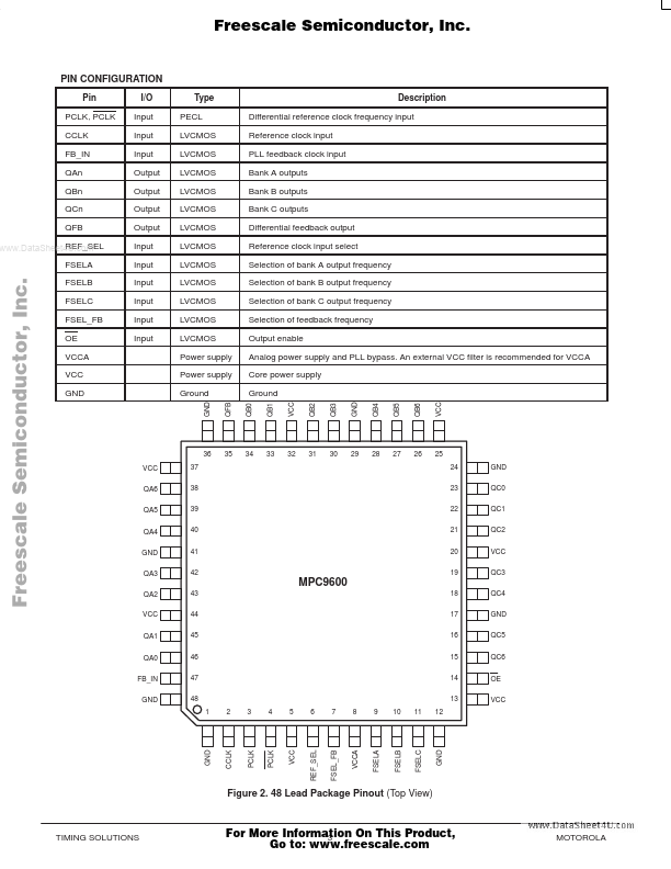
| Description | Differential reference clock frequency input Reference clock input PLL feedback clock input Bank A outputs Bank B outputs Bank C outputs Differential feedback output Reference clock input select Selec... |
| Features |
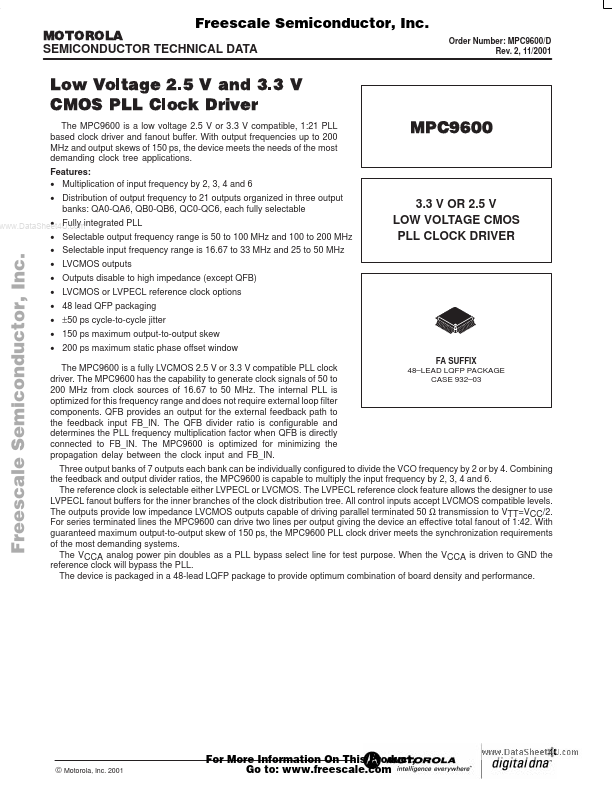
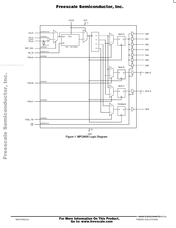
• Multiplication of input frequency by 2, 3, 4 and 6 • Distribution of output frequency to 21 outputs organized in three output banks: QA0-QA6, QB0-QB6, QC0-QC6, each fully selectable • Selectable output frequency range is 50 to 100 MHz and 100 to 200 MHz • Selectable input frequency range is 16.67 to 33 MHz and 25 to 50 MHz • LVCMOS outputs • Outputs disable to high impedance (except QFB) • LVCMOS or LVPECL reference clock options • 48 lead QFP packaging • ±50 ps cycle-to-cycle jitter • 150 ps maximum output-to-output skew • 200 ps maximum static phase offset window Order Number: MPC9600/D ... |
| Document |
PDF 365.84KB |
Similar Datasheet
| No. | Parte # | Fabricante | Descripción | Hoja de Datos |
|---|---|---|---|---|
| 1 | MPC9608 |

Motorola Inc |
1:10 LVCMOS Zero Delay Clock Buffer |

|
| 2 | MPC961C |

Motorola |
LOW VOLTAGE ZERO DELAY |

|
| 3 | MPC962305 |

Motorola |
(MPC962305 / MPC962309) Low-Cost 3.3 V Zero Delay Buffer |

|
| 4 | MPC962305 |

Renesas |
3.3V Zero Delay Buffer |

|
| 5 | MPC962308 |

Motorola |
3.3 V Zero Delay Buffer |

|
| 6 | MPC962309 |

Motorola |
(MPC962305 / MPC962309) Low-Cost 3.3 V Zero Delay Buffer |

|