Busque con el número de pieza junto con el fabricante o la descripción
NB6L11S |


| Part Number | NB6L11S |
| Manufacturer | ON Semiconductor (https://www.onsemi.com/) |
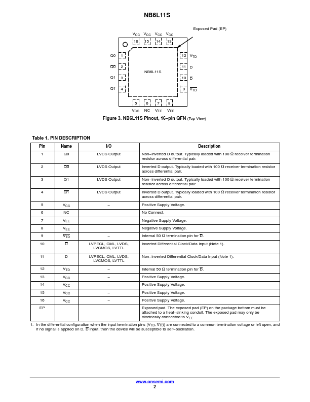
| Description | Pin Name I/O Description 1 Q0 LVDS Output Non−inverted D output. Typically loaded with 100 W receiver termination resistor across differential pair. 2 Q0 LVDS Output Inverted D output. Typ... |
| Features |
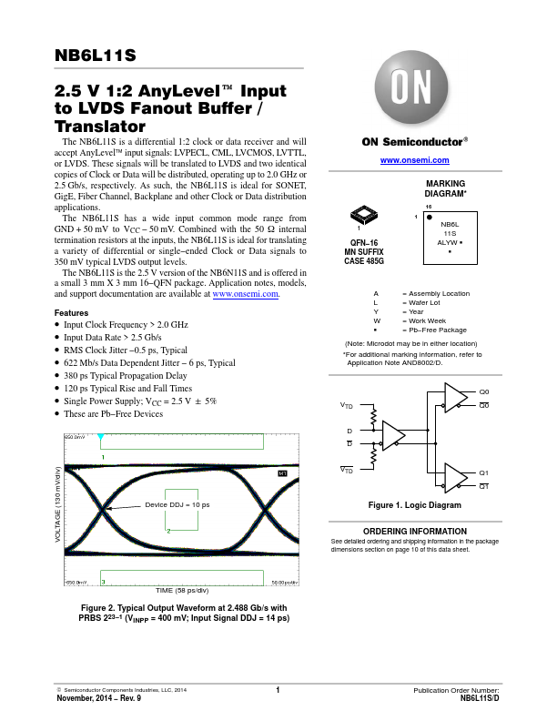
• Input Clock Frequency > 2.0 GHz • Input Data Rate > 2.5 Gb/s • RMS Clock Jitter −0.5 ps, Typical • 622 Mb/s Data Dependent Jitter − 6 ps, Typical • 380 ps Typical Propagation Delay • 120 ps Typical Rise and Fall Times • Single Power Supply; VCC = 2.5 V " 5% • These are Pb−Free Devices Device DDJ = 10 ps www.onsemi.com 1 QFN−16 MN SUFFIX CASE 485G MARKING DIAGRAM* 16 1 NB6L 11S ALYW G G A = Assembly Location L = Wafer Lot Y = Year W = Work Week G = Pb−Free Package (Note: Microdot may be in either location) *For additional marking information, refer to Application Note AND8002/D.... |
| Document |
PDF 316.46KB |
| No. | Parte # | Fabricante | Descripción | Hoja de Datos |
|---|---|---|---|---|
| 1 | NB6L11 |
ON Semiconductor |
2.5V / 3.3V MULTILEVEL INPUT TO DIFFERENTIAL LVPECL/LVNECL |

|
| 2 | NB6L11M |
ON Semiconductor |
Differential CML Fanout Buffer |

|
| 3 | NB6L14 |
ON Semiconductor |
Differential 1:4 LVPECL Fanout Buffer |

|
| 4 | NB6L14M |
ON Semiconductor |
Differential 1:4 CML Fanout Buffer |

|
| 5 | NB6L14S |
ON Semiconductor |
2.5V 1:4 AnyLevel Differential Input to LVDS Fanout Buffer/Translator |

|
| 6 | NB6L16 |
ON Semiconductor |
6GHz/6Gbps 2.5V/3.3V Multi-level Input to Differential Lvecl Clock or Data Translator/receiver/driver Buffer |

|