Busque con el número de pieza junto con el fabricante o la descripción
MN3890S |


| Part Number | MN3890S |
| Manufacturer | Panasonic Semiconductor |
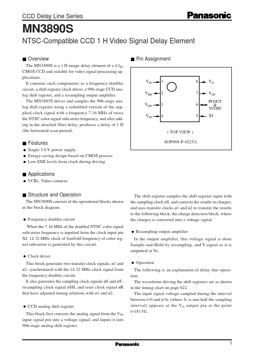
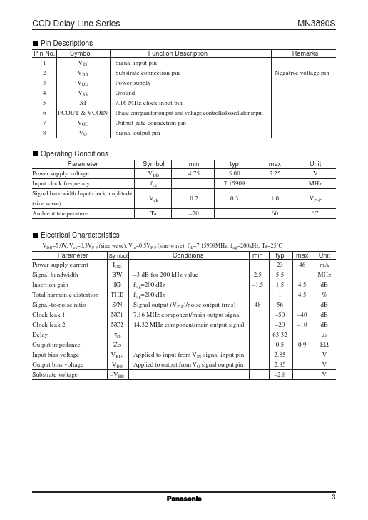
| Description | Pin No. 1 2 3 4 5 6 7 8 Symbol VIN VBB VDD VSS XI PCOUT & VCOIN VGC VO Function Description Signal input pin Substrate connection pin Power supply Ground 7.16 MHz clock input pin Phase comparator out... |
| Features |
Single 5.0 V power supply Energy-saving design based on CMOS process Low EMI levels from clock during driving
Applications
VCRs, Video cameras
Structure and Operation
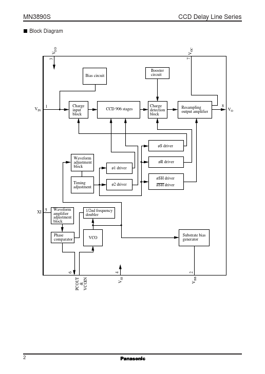
The MN3890S consists of the operational blocks shown in the block diagram. Frequency-doubler circuit When the 7.16 MHz of the doubled NTSC color signal subcarrier frequency is inputted from the clock input pin XI, 14.32 MHz clock of fourfold frequency of color signal subcarrier is generated by this circuit. Clock driver This block generates two transfer clock signals, ø1 and ø2, synchronized with the 14.32 MHz clock signal from... |
| Document |
PDF 53.10KB |
Similar Datasheet
| No. | Parte # | Fabricante | Descripción | Hoja de Datos |
|---|---|---|---|---|
| 1 | MN3814 |
Panasonic Semiconductor |
NTSC CCD Video Signal Delay Elements |

|
| 2 | MN3850 |

Micro Networks |
12-Bit D/A Converters |

|
| 3 | MN3860 |

Integrated Circuit Systems |
12-bit D/A Converter with Input Register |

|
| 4 | MN38662S |
Panasonic Semiconductor |
NTSC-Compatible CCD Video Signal Delay Element |

|
| 5 | MN38663S |
Panasonic Semiconductor |
NTSC-Compatible CCD Video Signal Delay Element |

|
| 6 | MN38664S |
Panasonic Semiconductor |
NTSC-Compatible CCD Video Signal Delay Element |

|